If you love science: this is a clean, scalable route to 2D amorphous matter on real device substrates. It removes the transfer step that often cracks or contaminates ultra-thin films, which has long clouded basic measurements.
If you don’t speak nanotech: think of building a house. Before, you had to make the walls on a metal sheet across the street and carry them over—often denting them. Now you can build right on the foundation, straighter and cleaner, with far fewer oops moments. That means faster research and, eventually, more reliable electronics made from exotic, atom-thin materials.
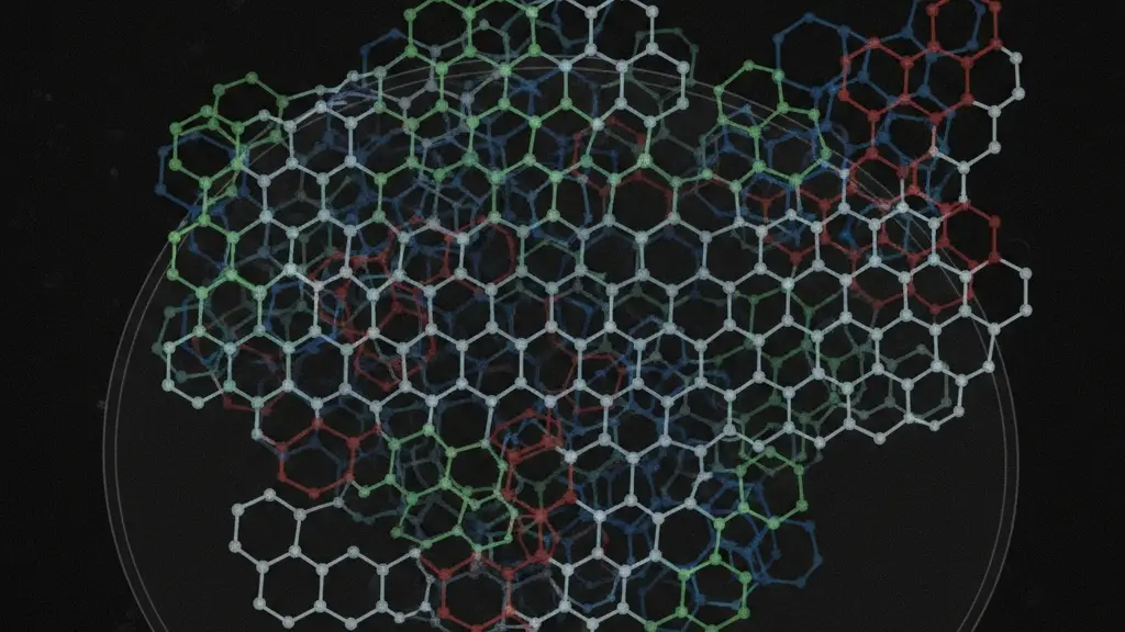
Quick background: What is monolayer amorphous carbon?
Unlike graphene (perfect hexagons), monolayer amorphous carbon is a single-atom-thick sheet where the carbon rings mix 5-, 6-, 7-, even 8-membered loops. It’s “vitreous” (glass-like), not crystalline—order in the small, disorder overall. Researchers first made free-standing monolayer a-C in 2019–2020, and later showed you can tune conductivity by changing the amount of structural disorder. The new work builds directly on that foundation, but crucially moves growth onto insulators at wafer scale.
The breakthrough: Tellurium-assisted 2D growth on insulators
Growing a-C on SiO₂/Si, sapphire, quartz—and covering a 2-inch wafer uniformly—required finesse. During chemical vapor deposition (CVD), the team introduced trace tellurium. Simulations and experiments agree: Te atoms transiently bridge the film edge to the substrate, suppressing out-of-plane buckling that would otherwise puff the film into a 3D foam. As growth proceeds, those weak Te bonds can break and reform, stabilizing a flat, continuous monolayer across the wafer. In short, Te acts like a gentle hand keeping the sheet flat while it expands.
Why that matters: Direct growth on insulators means no etching, no polymer residues, and no tears from transfers—so both basic physics measurements and device fabrication become far more trustworthy.
What they measured: Quantum tunneling at liquid-helium temperatures
Instead of fighting the film’s huge in-plane resistance at low temperature, the team measured out-of-plane tunneling through a device stack: Au / a-C / graphene. At 1.6 K, the current–voltage curves show linear behavior near zero bias (high resistance) transitioning to exponential tunneling at higher bias—classic insulating-barrier signatures. Moreover, multiple junctions on the same wafer behaved alike, indicating excellent uniformity. The device maps also lack phonon-tunneling “stripes” seen in crystalline hBN, reinforcing the amorphous (non-periodic) nature of the barrier.
Translation: at ultra-cold temps where quantum effects dominate, this ultrathin carbon acts like a good, even insulator, not a leaky mesh. That’s perfect for tunneling transistors, low-leakage dielectrics, and fundamental studies of electrons in disordered 2D systems.
What could this enable?
- Cleaner 2D device stacks: Direct-grown, patterned a-C as atom-scale insulators right on chips.
- Disorder-engineering tool: Combine with earlier work that tunes conductivity via disorder—now do it on real substrates and at scale.
- Quantum & neuromorphic devices: Use controllable tunneling and defect states as functional elements (e.g., selectors, memristive junctions).
For the science-curious: How Te really helps (the 30-second version)
At the growing edge of the carbon sheet, dangling bonds make the film want to curl and buckle (especially on weakly interacting SiO₂). DFT-informed kMC simulations show that Te atoms form temporary bridges between the film edge and the oxide surface. Those flexible bridges increase edge–substrate interaction, keeping the film flat and 2D while not permanently “locking” growth. Raise the growth temperature too high, and you start to crystallize nanographene, so they optimized ~650 °C to keep the film amorphous and uniform.
When will you see this in the wild?
Because the method is wafer-compatible and avoids transfers, it could enter research fabs immediately for 2D device prototyping. Industrial adoption depends on:
- scaling beyond 2-inch to standard wafers,
- process repeatability across tools, and
- long-term reliability data in device stacks. The path looks much smoother now than it did even a year ago.
Check out the cool NewsWade YouTube video about this article!
Sources
- Nature Communications (Oct 3, 2025): Tellurium-assisted growth of large-scale atom-thin insulating amorphous carbon on insulating substrates. (Wafer-scale growth on insulators; Te-assisted mechanism; low-T tunneling.) Nature
- Nature (Mar 2, 2023): Disorder-tuned conductivity in amorphous monolayer carbon. (Disorder control ↔ conductivity.) www2.coe.pku.edu.cn
- Nature (2020): Synthesis and properties of free-standing monolayer amorphous carbon. (First MAC synthesis.) ResearchGate