A New Way to See the Unseen
Scientists have developed a game-changing method to observe electron behavior in tiny, buried layers of advanced materials. This technique, called near-field fingerprint spectroscopy, uses light and cold temperatures to uncover how electrons move and gather in ultra-thin layers.
Why Does This Matter?
Today’s electronic devices rely on materials that are just atoms thick. Some of these systems, such as 2D electron gases (2DEGs), show unusual behaviors like superconductivity. However, understanding these behaviors requires tools that can see deep inside the material—without damaging it.
Until now, most tools could only give an unclear or indirect view. But this new approach, using a refined optical microscope at just 8 Kelvin (-265°C), lets scientists look directly into these buried layers.
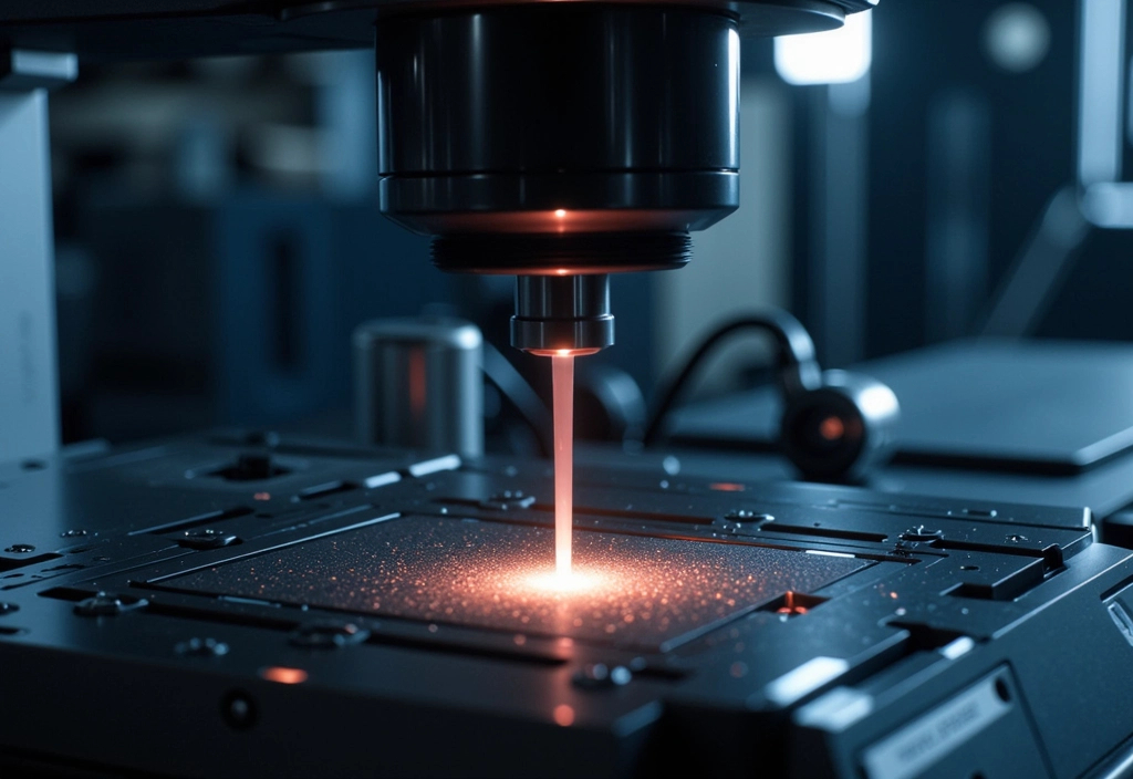
What the Researchers Did
The team focused on a well-known material: LaAlO₃/SrTiO₃ (LAO/STO). At the meeting point of these two materials, a special 2D electron system forms. This electron system is hard to study because it’s buried below the surface.
To solve this, researchers used a method called scattering-type scanning near-field optical microscopy (s-SNOM). They combined it with a powerful mid-infrared laser. This setup allowed them to detect unique “fingerprints” from the buried electrons. These signals changed depending on how many electrons were present and how freely they could move.
Importantly, they compared two nearly identical samples: one with the 2DEG and one without. This allowed them to isolate the signals coming specifically from the 2DEG, which was not possible before.
What They Found
The team identified three key peaks in the mid-infrared spectrum—between 700 and 900 cm⁻¹—that serve as a fingerprint of the 2DEG. These peaks respond in different ways depending on:
- Carrier concentration (how many electrons are packed in)
- Electron mobility (how freely those electrons can move)
By analyzing how each peak changed, the scientists could now separate the effects of each property. Previously, these effects were often tangled together, making analysis very difficult.
More Than Just One Material
This technique works beyond just LAO/STO. The team also tested it on doped indium arsenide (InAs), a material used in infrared sensors and transistors. They found that the fingerprint approach could also detect ultra-thin layers of extra electrons on the surface of InAs.
Therefore, the method is universal—it could apply to many systems including:
- Topological insulators
- Stacked 2D materials (like graphene)
- Other oxide interfaces
Real-World Uses
With this new tool, scientists can now:
- Map nanoscale defects in electronics
- Study how materials behave under stress or cold
- Improve designs for quantum and nano devices
Additionally, this method is non-destructive, meaning the same material can be reused or tested again.
Looking Ahead
This is just the beginning. As better infrared light sources become available, this technique will get even more powerful. Researchers plan to use it for studying how atomic defects or surface layers affect electron behavior in future materials.
By combining high-resolution imaging with this new spectral fingerprinting, engineers and physicists will gain deeper control over how advanced materials perform—leading to faster, smarter, and more efficient technology.
Check out the cool NewsWade YouTube video about this article!
Article derived from: Barnett, J., Wirth, K.G., Hentrich, R. et al. Low temperature near-field fingerprint spectroscopy of 2D electron systems in oxide heterostructures and beyond. Nat Commun 16, 4417 (2025). https://doi.org/10.1038/s41467-025-59633-1